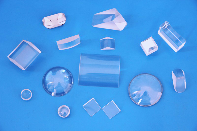
2'' 4'' 6'' semiconductor substrate/wafers,sapphire wafers
Sapphire semiconductor substrates are manufactured at Sapphire Products from high quality optical grade Czochralski sapphire. Our integrated facilities allow regulation of the production of substrates from crystal growth to fabrication, and to accommodate special requests on very short notice.
Sapphire semiconductor substrates are available in all orientations including R-axis (10-12), C-axis (0001), A-axis (11-20), and M-axis (11-10). Substrates are available in various shapes (circular, rectangle, or square), from a few mm up to 100mm in size, and finishes according to customer specification. Primary flats(as per industry standards) are provided on circular substrates for orientation purposes; secondary flats are available on request. Substrate thickness' range from 0.013" (0.25mm) to 0.025" (0.675mm), depending on your particular application requirements
Technical Parameters
2"Sapphire Wafers for LED Applications
|
Crystal
|
LED Grade Sapphire
|
|
Sapphire purity
|
99.996%
|
|
Orientation
|
C-Plane(0001) Off angle toward M-Axis0.2± 0.1°
|
|
C-Plane(0001)Off angle toward A-Axis0± 0.1°
|
|
Wafer Diamter
|
50.8± 0.1mm
|
|
Thickness
|
430±25um
|
|
Primary Flat
|
A-Plane(11-20)±0.25°
|
|
Flat Length
|
16±1mm
|
|
Front Side Surface Roughness
|
≤0.2nm
|
|
Back Side Surface Roughness
|
0.8~1.2um
|
|
TTV
|
≤5 um
|
|
LTV
|
≤2.0 (3um*3um)
|
|
TIR(Flatness)
|
≤3um
|
|
BOW
|
-10≤Bow≤10
|
|
Bubble & Color
|
None by visual inspection in intensive light
|
|
Ground Boundary
|
None by visual inspection in fluorescent light
|
|
Color
|
Transparent
|
|
Cleanliness
|
Epi-Ready
|
|
Package
|
Vacuum packed, in Class 100 clean romm, under a nitrogen atmosphere
|